After experiencing the pain of 10nm process dystocia, Intel 10nm-based Icelake Ice Lake processor finally opened the mysterious hijab.On August 1, the first batch of 11 (Sku) Icelake processor was officially announced:
Source: Intel
6 U series, 5 Y series.It is really time and again, it is actually Icelake is not the first generation of 10nm, CannonLake because of the problem on the process, only a small supply of low-end market, such as the low-end part of Lenovo.10nm dystocia cause I described in this article:
Wolf: Intel'S 10nm process CPU why not delay mass production?
zhuanlan.zhihu.com
Icon
If we ignore the failure of the test water, Icelake can be said to be high hopes, in this generation, the process and CPU architecture have made changes.With the announcement of the product, the change of Icelake is also disclosed:
- Source: Intel
f information in this page is very large, the other we will talk about in the future, this paper is more about the relationship architecture changes.The more technical details of Sunny Cove, the Icelake kernel architecture, are getting clearer and clearer, and today we'll look at what, for what, and how these changes affect the banchmark data.- Sunny Cove architecture
- Skylake can be said to be the longest-lived Intel architecture, since its appearance on the Skylake CPU, 4 years have only done a tinkering, fine-tuning and no essential changes.Previous generations of Nehalem, Sandybridge, haswell and other previous generations of tick, tock's rhythm was completely slowed down, into four generations of tick, tick, tick and tick.Finally this generation tock came, that is Sunny Cove new architecture.Unlike the previous Tock, this Tock also mixed with The Tick, the process of upgrading the architecture has also been upgraded.
- Source: Intel
- What changes did this new SunnyCove bring?Its schematics have been published:
- Source: Intel
- To sum up, it's the Deeper, the Wider and the Smarter.Smart refers to the branch predictor is improved, the architecture is relatively Skylake, it is more for the Client is the consumer market, rather than the server market, optimized.These are vague and do not tell the public details, because often involve trade secrets.Deeper and Wider have clear data support, which can also experience the exquisite design of the CPU.
- We zoom in this graph, first look at the CPU front end:
- Decent instruction decode line in the middle, you can see the 32KB instruction cache (I-cache) remains unchanged, decode or decode each clock cycle maximum 5 micro-ops, provided to the micro-ops queue (uop Queue).
Here to roughly explain what is micro-ops.Modern complex instruction set (CISC) CPU, borrowed from the reduced instruction set (RISC) idea, one instruction is disassembled into a number of RISC-like micro-operations: Micro-Ops.In this regard, CISC and RISC have been largely integrated.So how many micro-ops will each x86 instruction be broken down into?This is related to the complexity of the instruction, the instruction is simple even only one micro-ops, generally about 3, complex can be more than 4.
The part of Microcode is also unchanged and is also the largest offering of 4 micro-ops.The change is the right side of the micro-ops cache, its size from 1535 to 2304, expanded by 50%!It can provide 6 micro-ops to micro-ops queue.Increased micro-ops cache can provide faster micro-ops to the queue, which the depth of the queue made a request, on the other hand, micro-ops queue depth from 224, increased to 352, also increased by more than 50%.
Look at the CPU backend:
The larger queue with more Execute Port, EP from 8 to 10, is divided into 4 groups.4 ALU EP, 2 storage EP and 4 AGU EP.
More than a group of ALU EP to AVX-512, a total of two groups.Here to emphasize the AVX-512, although the server Xeon CPU on Skylake already support AVX-512, but on the Client side, this is the first generation support it (not short-lived CannonLake).AVX-512 vs. AVX-256 encryption and artificial intelligence, especially the recent hot Deep Learn is very helpful.Intel provides BL Boost library to developers, it can access Open Vino to provide transparent support, Press Here No table.
There is also a set of EP to AGU, used to do Store (store) AGU.Relative to Skylake 2 load, 1 store, now 2 load, 2 store.This is actually an optimization of the Client, increasing the store, rather than in the same way as the server emphasis on load.This relative L1 data cache (data cache) were increased from 32KB directly into the skylake 48KB, also increased by 50%.On the other hand, L2 cache doubled from 256KB became 512KB.
Some students see here that the original is to improve the performance of cache increases, so why not add more, is the cost of consideration?Not exactly, in fact, increase the Cache, because the index becomes large, the delay will increase accordingly, SunnyCove paid a price for this:
Source: Anandtech
L1 and L2 of Cache delay is increased.But increasing the delay at the same time, Cache because of the large hit rate will increase, which on the other hand will reduce the overall delay.So increase or decrease, increase the number of this architecture to carefully weigh.Obviously, SunnyCove architects believe that increasing the L1/L2 cache, despite the increase in their delay, but the overall performance of the system is still improved.
AnandTech website summed up a table, comparing the Intel generation, and AMD Zen direct comparison of these parameters, very direct and convenient:
Source: Anandtech
So Sunny Cove how much of these changes to improve performance?
Benchmark
According to Intel's official data, Icelake is up 18 percent from the Skylake IPC.%:
Here's the problem: Skylake is a 4-year-old CPU, averaging 4.5 percent a year if it's spread to 18 percent over four years.Not impressive.Is there more data?AnandTech made a detailed evaluation of the well-known hardware evaluation site[1].Relying on the popularity of the site, its editors were able to test the latest only 15W 1065G7:
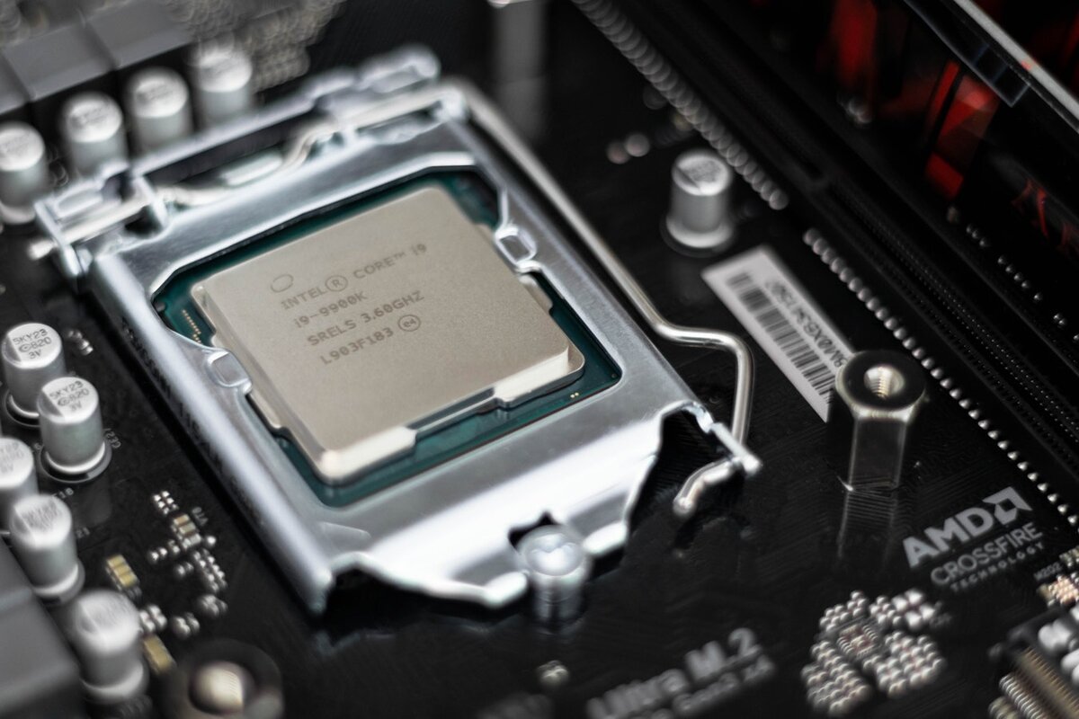
Test based on SPEC tests on CPU performance authority, compare 9900K and AMD 3900X.Details you can read reference 1, here only affixed to the overall score:
not like the previous generation?This is because 9900K TDP reached 95W, 15W of its direct fight performance was out of balance.Compared with the same power consumption of 8 generation 8550U can be seen clues, int 29% higher, floating-point 34% higher.Look at the Intel 18%is still relatively conservative.Let's take a look at the fairer per-GHz performance:
Results compared with 9900K, int increased by 14%.Overall, it increased by as much as 19 percent.
- Postscript
- Icelake's biggest improvement is its Gen11 built-in GPU, especially the sku with Iris.We'll talk about it next time.
- Other CPU hardware articles:
- Wolf: why the CPU frequency stop in 4G?Do we touch the frequency ceiling?
- Icon
- Wolf: one of those things CPU manufacturing:i7 and i5 is actually a twin brother!?
- Icon
- Wolf: CPU made those things two: Die size and yield
- Icon
- Wolf: why the wafer is not Round Square?
- Icon
- Wolf: why the "circuit" to be covered with the entire wafer?
- Icon
- Wolf: how long can the CPU work?Will it slow down because of aging?
- Icon
- Wolf: why is the CPU increasingly using silicone grease instead of solder heat?
- Icon
- Wolf: why the Intel CPU Die is getting smaller?
- Icon
- Wolf: cocoon of butterflies, from Ring Bus to Mesh network, the evolution of the CPU chip bus
- Icon
- Wolf: where is the 450mm wafer?
- Icon
- Wolf: what is TLB and PCID?Why have a PCID?Why does Linux start using it now?
- Icon
- Wolf: what is a Speculative Execution?Why have it?
- Icon
- Wolf:why not integrate the South Bridge into the CPU?What is the most precious resource of the CPU and the south bridge chip?
- Icon
- Wolf: what is the use of small CPU bottom?Why is the CPU so many power pins?
- Icon
- Wolf: TDP is the power consumption of the CPU?Is TDP fixed?
- Icon
- Welcome to pay attention to this column and use the WeChat scan below the two-dimensional code to join the WeChat public number"UEFIBlog", where there are the latest articles.